Solar cell
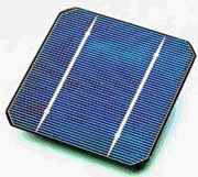
A solar cell or photovoltaic cell is a device that converts light energy into electrical energy. Sometimes the term solar cell is reserved for devices intended specifically to capture energy from sunlight, while the term photovoltaic cell is used when the light source is unspecified.
Fundamentally, the device needs to fulfill only two functions: photogeneration of charge carriers (electrons and holes) in a light-absorbing material, and separation of the charge carriers to a conductive contact that will transmit the electricity (simply put, carrying electrons off through a metal contact into a wire or other circuit). This conversion is called the photovoltaic effect, and the field of research related to solar cells is known as photovoltaics.
Solar cells have many applications. They have long been used in situations where electrical power from the grid is unavailable, such as in remote area power systems, Earth-orbiting satellites and space probes, consumer systems, e.g. handheld calculators or wrist watches, remote radiotelephones and water pumping applications. More recently, solar cells are starting to be used in assemblies of solar modules (photovoltaic arrays) connected to the electricity grid through an inverter, often in combination with a net metering arrangement.
Contents
Four generations of development
First
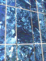
The first generation photovoltaic, consists of a large-area, single layer p-n junction diode, which is capable of generating usable electrical energy from light sources with the wavelengths of sunlight. These cells are typically made using a silicon wafer. First-generation photovoltaic cells (also known as silicon wafer-based solar cells) are the dominant technology in the commercial production of solar cells, accounting for more than 86% of the solar cell market.
Second
The second generation of photovoltaic materials is based on the use of thin-film deposits of semiconductors. These devices were initially designed to be high-efficiency, multiple-junction photovoltaic cells. Later, the advantage of using a thin-film of material was noted, reducing the mass of material required for cell design. This contributed to a prediction of greatly reduced costs for thin film solar cells. There are currently (2007) a number of technologies/semiconductor materials under investigation or in mass production. Examples include Amorphous silicon, Polycrystalline silicon, micro-crystalline silicon, Cadmium telluride, copper indium selenide/sulfide. Typically, the efficiencies of thin-film solar cells are lower compared with silicon (wafer-based) solar cells, but manufacturing costs are also lower, so that a lower cost per watt can be achieved. Another advantage of the reduced mass is that less support is needed when placing panels on rooftops and it allows fitting panels on light or flexible materials, even textiles.
Third
Third-generation photovoltaics are very different from the previous semiconductor devices as they do not rely on a traditional p-n junction to separate photogenerated charge carriers. These new devices include photoelectrochemical cells, polymer solar cells, and nanocrystal solar cells. Dye-sensitized solar cells are now in production.
Fourth
Fourth-generation composite photovoltaic technology with the use of polymers with nano particles can be mixed together to make a single multispectrum layer. Then the thin multispectrum layers can be stacked to make multispectrum solar cells more efficient and cheaper based on polymer solar cell and multi junction technology used by NASA on Mars missions. The layer that converts different types of light is first, then another layer for the light that passes and last is an infra-red spectrum layer for the cell — thus converting some of the heat for an overall solar cell composite.
Companies working on fourth-generation photovoltaics include Xsunx, Konarka Technologies, Inc., Nanosolar, Dyesol and Nanosys. Research is also being done in this area by the USA's National Renewable Energy Laboratory (http://www.nrel.gov/)
History
The term "photovoltaic" comes from the Greek φώς:phos meaning "light", and "voltaic", meaning electrical, from the name of the Italian physicist Volta, after whom the measurement unit volts are named. The term "photo-voltaic" has been in use in English since 1849.
The photovoltaic effect was first recognised in 1839 by French physicist Alexandre-Edmond Becquerel. However, it was not until 1883 that the first solar cell was built, by Charles Fritts, who coated the semiconductor selenium with an extremely thin layer of gold to form the junctions. The device was only around 1% efficient. Russell Ohl patented the modern solar cell in 1946 (U.S. Patent 2,402,662 , "Light sensitive device"). Sven Ason Berglund had a prior patent concerning methods of increasing the capacity of photosensitive cells. The modern age of solar power technology arrived in 1954 when Bell Laboratories, experimenting with semiconductors, accidentally found that silicon doped with certain impurities was very sensitive to light.
This resulted in the production of the first practical solar cells with a sunlight energy conversion efficiency of around 6 percent. This milestone created interest in producing and launching a geostationary communications satellite by providing a viable power supply. Russia launched the first artificial satellite in 1957, and the United States' first artificial satellite was launched in 1958. Russian Sputnik 3 ("Satellite-3"), launched on 15 May 1958, was the first satellite to use solar arrays. This was a crucial development which diverted funding from several governments into research for improved solar cells.
In 1970 first highly effective GaAs heterostructure solar cells were created by Zhores Alferov and his team in the USSR.
Applications and implementations
Solar cells are often electrically connected and encapsulated as a module. PV modules often have a sheet of glass on the front (sun up) side , allowing light to pass while protecting the semiconductor wafers from the elements (rain, hail, etc.). Solar cells are also usually connected in series in modules, creating an additive voltage. Connecting cells in parallel will yield a higher current. Modules are then interconnected, in series or parallel, or both, to create an array with the desired peak DC voltage and current.
The power output of a solar array is measured in watts or kilowatts. In order to calculate the typical energy needs of the application, a measurement in watt-hours, kilowatt-hours or kilowatt-hours per day is often used. A rule of thumb commonly used is that peak power times 20% gives average power, equating to one kW peak producing 4.8 kWh per day.
Theory
Simple explanation
- Photons in sunlight hit the solar panel and are absorbed by semiconducting materials, such as silicon.
- Electrons (negatively charged) are knocked loose from their atoms, allowing them to flow through the material to produce electricity. The complementary positive charges that are also created (like bubbles) are called holes and flow in the direction opposite of the electrons in a silicon solar panel.
- An array of solar panels converts solar energy into a usable amount of direct current (DC) electricity.
Optionally:
- The DC current enters an inverter.
- The inverter turns DC electricity into 120 or 240-volt AC (alternating current) electricity needed for home appliances.
- The AC power enters the utility panel in the house.
- The electricity is then distributed to appliances or lights in the house.
- The electricity that is not used will be re-routed and used in other facilities.
Photogeneration of charge carriers
When a photon hits a piece of silicon, one of three things can happen:
- the photon can pass straight through the silicon — this (generally) happens for lower energy photons,
- the photon can reflect off the surface,
- the photon can be absorbed by the silicon which either:
- Generates heat, OR
- Generates electron-hole pairs, if the photon energy is higher than the silicon band gap value.
Note that if a photon has an integer multiple of band gap energy, it can create more than one electron-hole pair. However, this effect is usually not significant in solar cells. The "integer multiple" part is a result of quantum mechanics and the quantization of energy.
When a photon is absorbed, its energy is given to an electron in the crystal lattice. Usually this electron is in the valence band, and is tightly bound in covalent bonds between neighboring atoms, and hence unable to move far. The energy given to it by the photon "excites" it into the conduction band, where it is free to move around within the semiconductor. The covalent bond that the electron was previously a part of now has one fewer electron — this is known as a hole. The presence of a missing covalent bond allows the bonded electrons of neighboring atoms to move into the "hole," leaving another hole behind, and in this way a hole can move through the lattice. Thus, it can be said that photons absorbed in the semiconductor create mobile electron-hole pairs.
A photon need only have greater energy than that of the band gap in order to excite an electron from the valence band into the conduction band. However, the solar frequency spectrum approximates a black body spectrum at ~6000 K, and as such, much of the solar radiation reaching the Earth is composed of photons with energies greater than the band gap of silicon. These higher energy photons will be absorbed by the solar cell, but the difference in energy between these photons and the silicon band gap is converted into heat (via lattice vibrations — called phonons) rather than into usable electrical energy.
Charge carrier separation
There are two main modes for charge carrier separation in a solar cell:
- drift of carriers, driven by an electrostatic field established across the device
- diffusion of carriers from zones of high carrier concentration to zones of low carrier concentration (following a gradient of electrochemical potential).
In the widely used p-n junction solar cells, the dominant mode of charge carrier separation is by drift. However, in non-p-n-junction solar cells (typical of the third generation of solar cell research such as dye and polymer thin-film solar cells), a general electrostatic field has been confirmed to be absent, and the dominant mode of separation is via charge carrier diffusion.
The p-n junction
The most commonly known solar cell is configured as a large-area p-n junction made from silicon. As a simplification, one can imagine bringing a layer of n-type silicon into direct contact with a layer of p-type silicon. In practice, p-n junctions of silicon solar cells are not made in this way, but rather, by diffusing an n-type dopant into one side of a p-type wafer (or vice versa).
If a piece of p-type silicon is placed in intimate contact with a piece of n-type silicon, then a diffusion of electrons occurs from the region of high electron concentration (the n-type side of the junction) into the region of low electron concentration (p-type side of the junction). When the electrons diffuse across the p-n junction, they recombine with holes on the p-type side. The diffusion of carriers does not happen indefinitely however, because of an electric field which is created by the imbalance of charge immediately either side of the junction which this diffusion creates. The electric field established across the p-n junction creates a diode that promotes current to flow in only one direction across the junction. Electrons may pass from the n-type side into the p-type side, and holes may pass from the p-type side to the n-type side. This region where electrons have diffused across the junction is called the depletion region because it no longer contains any mobile charge carriers. It is also known as the "space charge region".
Connection to an external load
Ohmic metal-semiconductor contacts are made to both the n-type and p-type sides of the solar cell, and the electrodes connected to an external load. Electrons that are created on the n-type side, or have been "collected" by the junction and swept onto the n-type side, may travel through the wire, power the load, and continue through the wire until they reach the p-type semiconductor-metal contact. Here, they recombine with a hole that was either created as an electron-hole pair on the p-type side of the solar cell, or swept across the junction from the n-type side after being created there.
Equivalent circuit of a solar cell
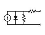
The equivalent circuit of a solar cell
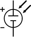
The schematic symbol of a solar cell
To understand the electronic behavior of a solar cell, it is useful to create a model which is electrically equivalent, and is based on discrete electrical components whose behaviour is well known. An ideal solar cell may be modelled by a current source in parallel with a diode; in practice no solar cell is ideal, so a shunt resistance and a series resistance component are added to the model. The resulting equivalent circuit of a solar cell is shown on the left. Also shown, on the right, is the schematic representation of a solar cell for use in circuit diagrams.
Solar cell efficiency factors
Maximum-power point
A solar cell may operate over a wide range of voltages (V) and currents (I). By increasing the resistive load on an irradiated cell continuously from zero (a short circuit) to a very high value (an open circuit) one can determine the maximum-power point, the point that maximizes V×I, that is, the load for which the cell can deliver maximum electrical power at that level of irradiation.
The maximum power point of a photovoltaic varies with incident illumination. For systems large enough to justify the extra expense, a maximum power point tracker tracks the instantaneous power by continually measuring the voltage and current (and hence, power transfer), and uses this information to dynamically adjust the load so the maximum power is always transferred, regardless of the variation in lighting.
Energy conversion efficiency
A solar cell's energy conversion efficiency (η, "eta"), is the percentage of power converted (from absorbed light to electrical energy) and collected, when a solar cell is connected to an electrical circuit. This term is calculated using the ratio of Pm, divided by the input light irradiance under "standard" test conditions (E, in W/m²) and the surface area of the solar cell (Ac in m²).
![]()
At solar noon on a clear March or September equinox day, the solar radiation at the equator is about 1000 W/m². Hence, the "standard" solar radiation (known as the "air mass 1.5 spectrum") has a power density of 1000 watts per square meter. Thus, a 12% efficiency solar cell having 1 m² of surface area in full sunlight at solar noon at the equator during either the March or September equinox will produce approximately 120 watts of peak power.
Fill factor
Another defining term in the overall behavior of a solar cell is the fill factor (FF). This is the ratio of the maximum power point divided by the open circuit voltage (Voc) and the short circuit current (Isc):
![]()
Quantum efficiency
Quantum efficiency refers to the percentage of absorbed photons that produce electron-hole pairs (or charge carriers). This is a term intrinsic to the light absorbing material, and not the cell as a whole (which becomes more relevant for thin-film solar cells). This term should not be confused with energy conversion efficiency, as it does not convey information about the power collected from the solar cell.
Comparison of energy conversion efficiencies
Solar cell efficiencies vary from 6% for amorphous silicon-based solar cells to 42.8% with multiple-junction research lab cells.[6] Solar cell energy conversion efficiencies for commercially available multicrystalline Si solar cells are around 14-16%. The highest efficiency cells have not always been the most economical — for example a 30% efficient multijunction cell based on exotic materials such as gallium arsenide or indium selenide and produced in low volume might well cost one hundred times as much as an 8% efficient amorphous silicon cell in mass production, while only delivering about four times the electrical power.
To make practical use of the solar-generated energy, the electricity is most often fed into the electricity grid using inverters (grid-connected PV systems); in stand alone systems, batteries are used to store the energy that is not needed immediately.
A common method used to express economic costs of electricity-generating systems is to calculate a price per delivered kilowatt-hour (kWh). The solar cell efficiency in combination with the available irradiation has a major influence on the costs, but generally speaking the overall system efficiency is important. Using the commercially available solar cells (as of 2006) and system technology leads to system efficiencies between 5 and 19%. As of 2005, photovoltaic electricity generation costs ranged from ~0.60 US$/kWh (0.50 €/kWh) (central Europe) down to ~0.30 US$/kWh (0.25 €/kWh) in regions of high solar irradiation. This electricity is generally fed into the electrical grid on the customer's side of the meter. The cost can be compared to prevailing retail electric pricing (as of 2005), which varied from between 0.04 and 0.50 US$/kWh worldwide. (Note: in addition to solar irradiance profiles, these costs/kwh calculations will vary depending on assumptions for years of useful life of a system. Most c-Si panels are warrantied for 25 years and should see 35+ years of useful life.)
Watts peak
Since solar cell output power depends on multiple factors, such as the sun's incidence angle, for comparison purposes between different cells and panels, the measure of watts peak (Wp) is used. It is the output power under these conditions known as STC:
- insolation (solar irradiance) 1000 W/m²
- solar reference spectrum AM (airmass) 1.5
- cell temperature 25°C
